DESCRIPTION
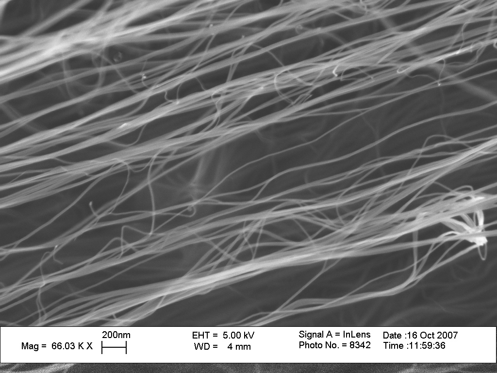
A bundle of singlewalled nanotubes processed into a thin sheet is shown in this scanning electron microscope image. Singlewalled nanotubes are extremely important in the continuing miniaturization of electronic devices. These tubes have an average diameter of 1-2 nm. Their electrical properties have led to their investigation as super capacitors for storing electrical charges. • SIZE: The thickness of the sheet is about 50 µm. • IMAGING TOOL: Scanning electron microscope

DESCRIPTION
A bundle of singlewalled nanotubes processed into a thin sheet is shown in this scanning electron microscope image. Singlewalled nanotubes are extremely important in the continuing miniaturization of electronic devices. These tubes have an average diameter of 1-2 nm. Their electrical properties have led to their investigation as super capacitors for storing electrical charges. • SIZE: The thickness of the sheet is about 50 µm. • IMAGING TOOL: Scanning electron microscope
OBJECTIVES
NANO CONTENT MAP
Nanometer-sized things are very small, and often behave differently than larger things do.
Nanoscience, nanotechnology, and nanoengineering lead to new knowledge and innovations that weren't possible before.
Credits
Mei Zhang, University of Texas at Dallas - Attribution is required. The creator listed here has made this image available to NISE Network partners for non-profit educational use only. Uses may include but are not limited to reproduction and distribution of copies, creation of derivative works, and combination with other assets to create exhibitions, programs, publications, research, and websites.
The creator listed above has made this image available to NISE Network partners for non-profit educational use only. Uses may include but are not limited to reproduction and distribution of copies, creation of derivative works, and combination with other assets to create exhibitions, programs, publications, research, and websites.